Single layer single crystal graphene suitable for various types of sensors
Scientists studied a true single layer, that is, a large area graphene film covered on a large area of copper foil. Improved chemical vapor deposition (CVD) growth method, eliminating all the carbon impurities of graphene growth on copper foil.
This uniform "perfect" single-layer single-crystal graphene is expected to be used as an ultra-thin support material for ultra-high resolution transmission electron microscope imaging and optical equipment. It can also be used as a suitable graphene to achieve very uniform functionalization, which will promote many other applications, especially for various types of sensors.

Director Rodney Ruoff of the Center for Multidimensional Carbon Materials (CMCM) from the Institute of Basic Science (IBS) of the Ulsan National Institute of Science and Technology (UNIST), led the research team. This seems to be the latest in a series of similarities about single-layer graphene. However, the difference between this result and thousands of previous papers is that none of them really describe large-area single-layer graphene, and Adlayers (double-layer or multi-layer regions) have always existed. IBS scientists have improved the chemical vapor deposition (CVD) growth method to eliminate all carbon impurities that graphene grows on copper foil.
Chemical vapor deposition (CVD) on metal foil (especially copper foil) is currently the most promising method for preparing large-area high-quality graphene films. The research team studied why "adlayers" appear in graphene films grown on copper foil, and found that carbon impurities in the films directly lead to the nucleation and growth of adlayers. Through the use of time-of-flight secondary ion mass spectrometry and combustion analysis, it is found that commercial copper foil has'excess carbon', especially near the surface, with a depth of about 300 nanometers. After discussing with a technical expert from Jiangxi Copper Co., Ltd., one of the largest copper foil suppliers in the world, the researchers learned:
In the production process, carbon is embedded in the copper foil, possibly from the hydrocarbon-based oil used to lubricate the rolls that the copper foil contacts during high-temperature rolling. After the carbon is completely removed under the condition of the H2 temperature of 1060°C, no adlayfree can be achieved, thereby realizing a true single-layer graphene film. Through the same method, IBS scientists also obtained adlayer-free single-layer and single-crystal graphene films on single-crystal copper foil. Wang Meihui (transliteration), one of the first authors of the study, explained: In this way, we have solved two problems that have always existed in the simultaneous synthesis of CVD graphene films (adlayers and grain boundaries, GBs). Indeed, achieving perfect uniformity of the number of layers on a large area (such as a single layer or double layer) can be used to ensure the uniformity of equipment performance.
The difference in the Adlayer area is that when it exists in the active area of the device, the density and size of the Adlayer area are also different. In addition to adlayers, GBs also exist in polycrystalline graphene films prepared by CVD, where graphene islands with different crystal orientations are connected together to form a film. The existence of GBs reduces the carrier mobility and thermal conductivity, and reduces the mechanical strength. Nonetheless, the scientists left a fascinating feature on the single crystal film: This single crystal graphene contains highly oriented parallel "folds" measuring centimeters in length and 100 nanometers in width at intervals of 20 to 50 microns. Like adlayers and GBs, wrinkles can significantly reduce the carrier mobility of graphene.
In order to eliminate the scattering effects of adlayers, GBs and wrinkles, the research team drew the field-effect transistor pattern in the area between two adjacent wrinkles and on the transistors parallel to the wrinkles. Unlike the quasi-randomly distributed wrinkles in polycrystalline graphene films, the wrinkles are highly arranged in a large area single crystal graphene film. This makes it easy to manufacture integrated high-performance devices from the area between the folds. The area between two adjacent folds is ‘clean’ without any folds, adlayers or GBs, which gives the device high electron and hole mobility.
Field effect transistors show very high room temperature carrier mobility values of approximately 1.0 x 104 cm2V-1s-1. Such high carrier mobility "transforms" into various useful devices with high performance. The development of large-area adlayer-free single crystal graphene is a breakthrough. This uniform and "perfect" single-layer single-crystal graphene is expected to be used as an ultra-thin support material for ultra-high-resolution transmission electron microscopy imaging and optical equipment. It can also be used as a suitable graphene to achieve very uniform functionalization.
Link to this article: Single layer single crystal graphene suitable for various types of sensors
Reprint Statement: If there are no special instructions, all articles on this site are original. Please indicate the source for reprinting:https://www.cncmachiningptj.com
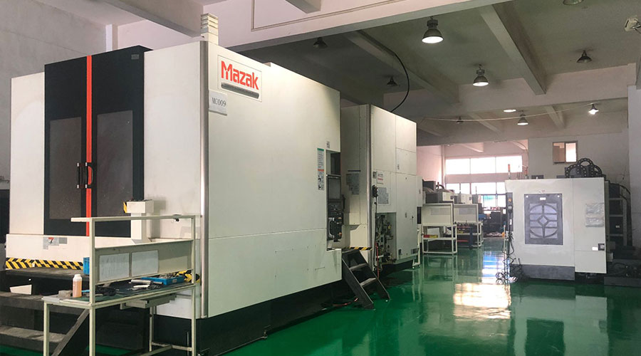 PTJ® provides a full range of Custom Precision cnc machining china services.ISO 9001:2015 &AS-9100 certified.
Machining shop specializing in fabrication services for construction and transportation industries. Capabilities include plasma and oxy-fuel cutting, Tailored machining, MIG and Custom Aluminum Cnc Precision Milling Welding Jig Fixture, roll forming, assembly, Lathe machining stainless steel cnc machine shaft, shearing, and CNC Swiss Machining services. Materials handled include carbon and Passivation Stainless Steel Machining Cover Plate Parts.
Tell us a little about your project’s budget and expected delivery time. We will strategize with you to provide the most cost-effective services to help you reach your target,You are welcome to contact us directly ( [email protected] ) .

- 5 Axis Machining
- Cnc Milling
- Cnc Turning
- Machining Industries
- Machining Process
- Surface Treatment
- Metal Machining
- Plastic Machining
- Powder Metallurgy Mold
- Die Casting
- Parts Gallery
- Auto Metal Parts
- Machinery Parts
- LED Heatsink
- Building Parts
- Mobile Parts
- Medical Parts
- Electronic Parts
- Tailored Machining
- Bicycle Parts
- Aluminum Machining
- Titanium Machining
- Stainless Steel Machining
- Copper Machining
- Brass Machining
- Super Alloy Machining
- Peek Machining
- UHMW Machining
- Unilate Machining
- PA6 Machining
- PPS Machining
- Teflon Machining
- Inconel Machining
- Tool Steel Machining
- More Material

