Application of Photoforming Technology in Micromachining
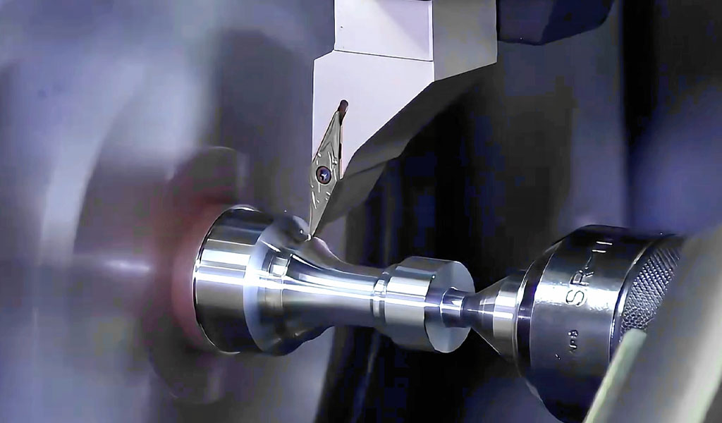
Photoforming technology, a subset of photolithography-based fabrication methods, has emerged as a crucial technique in the realm of micro-machining. This article explores the application of photoforming technology in micro-machining, emphasizing its advantages, technical processes, and comparative performance against traditional methods. The discussion extends to material compatibility, precision, scalability, and industrial applications, supplemented with detailed comparative tables.
Introduction to Photoforming Technology
Photoforming technology involves the use of light-sensitive materials and photochemical reactions to achieve high-precision microstructures. It is particularly relevant in micro-machining due to its ability to produce intricate designs with sub-micron accuracy. The process is commonly utilized in micro-electromechanical systems (MEMS), semiconductor fabrication, and high-precision industrial components.
Fundamental Principles of Photoforming
Photoforming is based on photopolymerization, where ultraviolet (UV) or laser light selectively hardens or alters the properties of a photosensitive material. The primary steps include:
-
Exposure: A photomask or direct laser writing is used to expose specific regions of a photoresist.
-
Development: The exposed or unexposed areas (depending on the resist type) are removed, revealing the desired pattern.
-
Etching or Deposition: The developed pattern serves as a template for further processing, such as metal deposition, electroforming, or chemical etching.
Applications of Photoforming Technology in Micro-Machining
Micro-machining requires extreme precision, making photoforming technology a suitable approach. Below are key application areas:
1. Semiconductor Industry
The semiconductor industry extensively utilizes photoforming for micro-patterning on silicon wafers. The technique is essential in:
-
Integrated Circuit (IC) Fabrication: Creating nanometer-scale transistor architectures.
-
Photomask Production: High-precision masks for lithographic processes.
-
Wafer-Level Packaging: Forming micro-scale interconnections.
2. Microfluidics
Photoforming is a preferred method for microfluidic device fabrication, offering benefits such as:
-
High Aspect Ratio Structures: Enables the creation of deep microchannels.
-
Material Versatility: Compatible with polymers, glass, and silicon.
-
Mass Production Potential: Allows batch processing for cost efficiency.
3. Biomedical Devices
Micro-machined structures via photoforming find applications in medical and biomedical fields:
-
Lab-on-a-Chip Devices: Miniaturized diagnostic tools with intricate fluidic networks.
-
Microneedles: Drug delivery systems with precision-controlled penetration depths.
-
BioMEMS: Biocompatible microelectromechanical systems for cellular research.
4. Optoelectronics
Precision optics benefit from photoforming in:
-
Microlens Arrays: Fabrication of high-resolution optical elements.
-
Waveguides: Controlled propagation of light for fiber-optic communication.
-
Diffractive Optical Elements (DOEs): High-precision diffraction gratings.
5. Aerospace and Defense
High-precision micro-components are integral in aerospace applications, including:
-
Micro-Turbine Blades: Lightweight structures with complex geometries.
-
Sensor Arrays: Highly accurate positioning and detection modules.
-
MEMS Inertial Sensors: Gyroscopes and accelerometers for navigation.
Comparative Analysis: Photoforming vs. Traditional Micro-Machining Techniques
Below is a comprehensive comparison between photoforming and conventional micro-machining methods such as CNC micromachining, laser ablation, and electrochemical etching.
| Attribute | Photoforming Technology | CNC Micro-Machining | Laser Ablation | Electrochemical Etching |
|---|---|---|---|---|
| Feature Size | Sub-micron resolution | Limited by tool size | Micron-level | Micron-level |
| Material Versatility | High (metals, polymers, glass) | Limited to machinable materials | Wide range | Metals only |
| Aspect Ratio | High | Moderate | High | Moderate |
| Batch Processing | Yes | No | Limited | Yes |
| Cost Efficiency | High for large volumes | Expensive for micro parts | Moderate | High for mass production |
| Scalability | Excellent | Poor | Moderate | High |
| Tool Wear | None | High | None | None |
Advantages and Limitations of Photoforming Technology
Advantages
-
Extreme Precision: Capable of sub-micron feature sizes.
-
Material Flexibility: Can be applied to metals, ceramics, and polymers.
-
Scalability: Effective for both prototyping and large-scale manufacturing.
-
Non-Contact Process: Eliminates tool wear and mechanical stress on parts.
Limitations
-
Process Complexity: Requires precise control over photopolymerization parameters.
-
Material Restrictions: Not all materials are photoresponsive.
-
High Initial Setup Cost: Photolithographic equipment is expensive.
Future Prospects and Innovations
Advancements in photoforming technology continue to enhance micro-machining capabilities. Emerging trends include:
-
3D Photoforming: Multi-layer photopolymerization for complex 3D microstructures.
-
Nano-Scale Lithography: Further miniaturization for next-generation semiconductors.
-
Hybrid Manufacturing: Combining photoforming with additive manufacturing techniques.
Conclusion
Photoforming technology stands as a transformative approach in micro-machining, offering unmatched precision, scalability, and material versatility. Its applications span across multiple industries, from semiconductors to biomedical engineering, making it a cornerstone of modern high-precision manufacturing.
The continuous evolution of photopolymerization techniques and material science will further enhance the capabilities of photoforming technology, solidifying its role in the future of micro-machining.
Reprint Statement: If there are no special instructions, all articles on this site are original. Please indicate the source for reprinting:https://www.cncmachiningptj.com/,thanks!
 3, 4 and 5-axis precision CNC machining services for aluminum machining, beryllium, carbon steel, magnesium, titanium machining, Inconel, platinum, superalloy, acetal, polycarbonate, fiberglass, graphite and wood. Capable of machining parts up to 98 in. turning dia. and +/-0.001 in. straightness tolerance. Processes include milling, turning, drilling, boring, threading, tapping, forming, knurling, counterboring, countersinking, reaming and laser cutting. Secondary services such as assembly, centerless grinding, heat treating, plating and welding. Prototype and low to high volume production offered with maximum 50,000 units. Suitable for fluid power, pneumatics, hydraulics and valve applications. Serves the aerospace, aircraft, military, medical and defense industries.PTJ will strategize with you to provide the most cost-effective services to help you reach your target,Welcome to Contact us ( [email protected] ) directly for your new project.
- 5 Axis Machining
- Cnc Milling
- Cnc Turning
- Machining Industries
- Machining Process
- Surface Treatment
- Metal Machining
- Plastic Machining
- Powder Metallurgy Mold
- Die Casting
- Parts Gallery
- Auto Metal Parts
- Machinery Parts
- LED Heatsink
- Building Parts
- Mobile Parts
- Medical Parts
- Electronic Parts
- Tailored Machining
- Bicycle Parts
- Aluminum Machining
- Titanium Machining
- Stainless Steel Machining
- Copper Machining
- Brass Machining
- Super Alloy Machining
- Peek Machining
- UHMW Machining
- Unilate Machining
- PA6 Machining
- PPS Machining
- Teflon Machining
- Inconel Machining
- Tool Steel Machining
- More Material

